Thursday 27 July 2017

What are IP Ratings

In the wonderful world of engineering standards, BS EN 60529:1992 is probably one of the most used in electronic and electrical engineering. Any time an electrical product is sold within some sort of enclosure, it will have an IP rating associated with it. The standard defines what environments the enclosure can protect the electronics inside it from. IP comes from the french term Indice de Protection which translates to the Protection Factor. Basically, the higher the numbers, the more protection it can afford against dust and liquid.

An IP rating consists of the letters "IP" followed by two single digits. Using IPXY, X denotes protection from solid particles, like dust or fingers; and Y denotes protection from liquids, water being the most common test. The enclosure must be able to operate normally whilst being subjected to the rated (in the tables below) for no more than 30 minutes.

X
Description
0 No protection
1 Protection against objects larger than 5cm
2 Protection against objects larger than 1.25cm (e.g fingers)
3 Protection against objects larger than 1.25cm (e.g wires/screwdrivers)
4 Protection against objects larger than 1mm (e.g insects)
5 Protection against dust
6 Dust tight

Y
Description
0 No protection
1 Dripping water
2 Dripping water at an angle
3 Falling water
4 Water splashes
5 Water jet
6 Powerful water jet
7 Immersion < 1m
8 Immersion > 1m
9 High pressure, high temperature water jet

These ratings have been seen recently in the latest Apple and Samsung smartphones. The IPhone 7 claims IP67, so dust tight, and waterproof to less than 1m. Samsungs S8 is rated at a high IP68, so it is dust tight and waterproof over 1m. Equally, if you have a device that like a mains plug, it has big holes in it where it fits into the other plug. These holes won't stop dust, and definitely don't stop water in any form, but it will stop you putting your fingers inside it. These sort of devices are rated as IP2X, with the X meaning it could be any form of waterproof, but it is untested.

It is important to note that sometimes a device can have a dual rating. Due to the way that the liquid protection scale works, you could in theory have a device that can withstand immersion more than 1m (IPX8), but fails to stop water jets. So sometimes you will get manufacturers specifying that is can withstand one or the other to stop confusion.

The ratings for water immersion are also very vague, when underwater, pressures can change and increase massively depending on the movements of the device. If it is a watch, it can be put under huge pressures if the user starts swimming with it. Even if it is rated to immersion <1m, that movement could put the device at a much higher pressure, as if it is much deeper underwater. This is why some devices like smart watches are IP67 rated, but call themselves "splash resistant" rather than water resistant.

Friday 30 June 2017

My 4 Bit Ripple Carry Adder/Subtractor Project

After creating my 1 bit full adder design found in a previous post, I decided to go for something a little more complicated. I wanted to prove to myself that the ripple carry system worked, so the obvious choice is to make a multi bit device. 4 bits seemed like a good amount, it's a value used in some early ALU's so it can be used in a future project. To make it more interesting I added in the ability to make the device a Subtractor at the same time. When you look at the schematic, it only requires one more device per adder, so it's not even an expensive thing to implement, but adds lots of functionality. As with the 1 bit adder, I have attempted to build this adder using only single logic chips.


The first stage is to know the logic circuit, its widely known and can be found pretty easily all over the web. Im not going to explain how it's created (I can always make a separate post on that) but I can describe how to use it. The aim is for the device to take two 4 bit inputs (0 - 15), along with a carry from another adder. So the adder needs to be able to output a value between 0 and 31. In binary this can be shown as 5 bits, so we have 2 outputs. This the S output is a 4 bit bus, and the Co output bumps this up to the 5 bits we need to make 31. A truth table can be made for this but it would be 32 lines long, so too much for this post. You could regard it as a personal challenge if you want to attempt it on your own.

So I got onto Altium and made a schematic of this circuit using some of the low voltage 7400 LVC series individual logic gates that I used on the previous adder I made. They come in SOT23-5 packages which are leaded a nice size to solder. Plus they are a size where it's possible to probe the pins fairly easily. Luckily Altium shows the components as their logic symbols. Below I have shown the first two adders, the third and fourth are basically the same as the second one, which is the idea of the ripple carry adder.

The first two adders of the four found on the board

I also added a few LEDs to show what parts are on and off. This means the user can see the inputs and outputs. These LEDs run off the 5V input voltage, and have 220Ω current limiting resistors in series with them. Also, I have put in some 0.1 inch header pins so it can be attached into a breadboard and maybe even a micro.

The LEDs for the carry bits and outputs

The LEDs for the input bits

As a base of my circuit, I have decided on a double sided 100mm x 100mm board. This is quite big as you can see for the circuit I have made, but gives plenty of space for a soldering iron to get access. As well as this, it gives a nice amount of space for multimeter probes. I also tried to keep the individual logic chips in a similar arrangement as the schematic. This is meant to be used as a learning device, so it's useful for the chips to line up with the diagram. The header pins for the inputs and outputs are placed on opposite sides of the board to make it more obvious for the user to see it. And the pins have designators written on the board so the user can see what each pin does. The input and output busses are placed in fairly logical places, and grouped together. There is no point having all the A inputs intertwined with the B inputs. The pins for the power and ground are on opposite sides with their own headers, only one needs to be connected for it to work. The LEDs that are directly attached to the pins are placed closer to the logic circuitry, but labeled clearly on the silkscreen. Most of the routing to the LEDs is on the underside of the board, else the top could get confusing. All the designators for components have been made half the normal size due to the small amount of parts used in the project. The below images show the PCB layout I created with the top copper being red, bottom copper being blue, and the silkscreen shown in yellow.

Top Copper

As you might be able to see, I have tried to keep all the power on the bottom side of the board. This leaves lots of space for the logic signals on the top, where the user is more likely to see. As you can see, most of the inputs and outputs of the circuit are also on the bottom side. This is because the way the busses work  and input into the adder needs lots of crossing over and would add confusion into the design. This is why labels were used instead.

Bottom Copper
To make it easier to see, I made a larger image of the first and last adder in the series. As you can see, the only real difference in them is that the first has the add/subtract input shown by an LED, whereas the last shows the carry from the previous adder (C0). This is because the A/D bit is attached to all the adders, but the first bit doesn't have a carry bit input. The carry on that adder is the input for the A/S. It serves the function of inverting the first bit, so that it works like 2's complement when in subtract mode.

The layout of the first adder in the series

The layout of the last adder in the series

As noted above I used 7400 LVC series logic gates. The SOT23-5 package chips have the suffix of "BVD". See the datasheets for each of the devices for more information. I have written a simple bill of materials below:

  • 12x SN74LVC1G86DBVT - XOR gate
  • 8x SN74LVC1G08DBVT - AND gate
  • 4x SN74LVC1G32DBVT - OR gate
  • 17x DO-214 LED's
  • 17x 0805 220Ω resistors
  • 6x 5-pin 0.1" header pins
The main downside to this type of adder is that is is very slow. Especially when you get to high bit amounts that you are trying to add. This adder will take at least 4 times as long as a single adder to add the two numbers together. This problem is known as propagation delay, each logic chip will take a very short time to compute the output. Although this time is not perceivable by the human eye, if there are 100's of logic gates in a row, then the delays start to add up and be a problem. If this circuit is to be used in a computer, it could need to make calculations thousands, or maybe millions of times a second, and a carry bit adder is not generally good at that. There are other, faster adders that I will show in a future post.

Friday 9 June 2017

My 1 Bit Full Adder Project

One thing that has always been interesting to me is using logic circuitry in electronics. Its easy to implement something on a microcontroller in just a few lines, but where the real challenge comes from is making a boolean project using real logic gates. It's something we all learn about if you have taken a basic computer science class, or even sometimes in digital electronics. One of the first circuit's you ever learn about is the adder. Its pretty simple, teaches you how to cancel down boolean equations, and only has a few inputs and outputs. I have decided to try and make the circuit using real components, and see if I can get it to work.

The first stage is to know the logic circuit, its widely known and can be found pretty easily all over the web. Im not going to explain how it's created (I can always make a separate post on that) but I can describe how to use it. The aim is for the device to take two 1 bit inputs, along with a carry from another adder. So the adder needs to be able to output a value between 0 and 3. In binary this can be shown as 2 bits, so we have 2 outputs. This the S output represents a 1, and the Co output represents bit 2. Below is the truth table I used, if you want a little challenge, try and get the above circuit using boolean algebra.

A
B
Ci
Co
S
0
0
0
0
0
0
0
1
0
1
0
1
0
0
1
0
1
1
1
0
1
0
0
0
1
1
0
1
1
0
1
1
0
1
0
1
1
1
1
1

So I got onto Altium and made a schematic of this circuit using some of the low voltage 7400 LVC series individual logic gates. They come in SOT23-5 packages which are leaded a nice size to solder. Plus they are a size where it's possible to probe the pins fairly easily. Luckily Altium shows the components as their logic symbols.


I also added a few LEDs to show what parts are on and off. This means the user can see the inputs and outputs. These LEDs run off the 5V input voltage, and have 220Ω current limiting resistors in series with them. Also, I have put in some 0.1 inch header pins so it can be attached into a breadboard and maybe even a micro.


As a base of my circuit, I have decided on a double sided 50mm x 50mm board. This is quite big as you can see for the circuit I have made, but gives plenty of space for a soldering iron to get access. As well as this, it gives a nice amount of space for multimeter probes. I also tried to keep the individual logic chips in the same arrangement as the schematic. This is meant to be used as a learning device, so it's useful for the chips to line up with the diagram. The header pins for the inputs and outputs are placed on opposite sides of the board to make it more obvious for the user to see it. The pins for the power and ground are on the same side on both headers. The LEDs that are directly attached to the pins are kept close to them, and the track is fairly obvious to show where the signal is from. The silkscreen labels which LED designates which input/output. All the designators have been made half the normal size due to the small amount of parts used in the project. The below images show the PCB layout I created with the top copper being red, bottom copper being blue, and the silkscreen shown in yellow.

Top Copper
As you might be able to see, I have tried to keep all the power on the bottom side of the board. This leaves lots of space for the logic signals on the top, where the user is more likely to see. As you can see, not all signals are on the top side due to circuit constraints,  but signals that do swap over are generally short jump, and straight lines, This makes it more obvious where the tracks go without having to flip the board. 

Bottom Copper
As noted above I used 7400 LVC series logic gates. The SOT23-5 package chips have the suffix of "BVD". See the datasheets for each of the devices for more information. I have written a simple bill of materials below:

  • 2x SN74LVC1G86DBVT - XOR gate
  • 2x SN74LVC1G08DBVT - AND gate
  • 1x SN74LVC1G32DBVT - OR gate
  • 5x DO-214 LED's
  • 5x 0805 220Ω resistors
  • 2x 5-pin 0.1" header pins

Tuesday 6 June 2017

How a Voltage Regulator Works: LM7805

Voltage regulators are one of the first electronic components used by a hobbyist. It simply takes a voltage that is too high, and reduces it down to a set voltage that you want. Sounds like a great solution, but there is an issue, they are terribly inefficient. They are known to get very hot when used at high currents, and often need hefty heatsinks to stop the magic smoke from being released. To demonstrate why they get so hot we need to think about what happens during use. Remembering Kirchoff, the current going into a system is the same as the current going out of the system. If we use a simplified version of the regulator, the only thing this device changes is the voltage of the output. Due to the minimal current lost powering the circuit we assume the vast majority of power lost is in heat. Using the basic equation of:

Power (W) = Voltage (V) x Current (I)

So if we use an example of the LM7805 made by On Semiconductor (previously Fairchild) that can regulate 5V at 1A. Its a pretty standard component, and is very typical of a voltage regulator.

If we use a 9V input the power going in is 9V x 1A = 9W.

The output power is 5V x 1A = 5W.

This means that there is 4W of power being dissipated from the regulator as wasted heat. This is a large amount when considering the size of the packages available. When thinking about problems excessive heat can cause in a circuit, it can quite easily damage itself and other components around it when not designed properly. 

This post isnt meant to dissuade you from using regulators, they have their place in electronic circuits, and are a great starting point. All electronic engineers need to have a broad understanding of the advantages and disadvantages of linear voltage regulators to be able to handle them properly.

How it Works


The above schematic can be found on the datasheet, but it's been coloured in to show the different sections of the circuit.

The most important component in the above schematic is Q16 (Red), it controls the current between the input and output, therefore the voltage. It is placed in a darlington pair configuration with Q15 (Orange). In this configuration Q16 is amplifying the current amplified by Q15. This means that Q15 can be used to introduce error feedback. The Blue section contains a voltage divider that scales the output voltage so that it can be used by the bandgap circuit. This bandgap circuit is found in the yellow section (Q1 and Q6). This bandgap reference produces an error signal that is fed into Q7 (orange). A bandgap is used because it can provide a stable output even when the temperature of the device changes.

The orange section takes this error and amplifies it through Q15 and the darlington configuration described earlier. The purple section has overheating protection (Q13) and excessive output current protection (Q14). Occasionally on these schematics you also find excessive input voltage protection marked as Q19 in this section. These shutdown the regulator in fault conditions like overcurrent or getting too hot. The Green section is known as the "start up" circuit, because it provides the initial current needed to power the bandgap circuitry. This gives a jumpstart to the circuit when it needs it.

I chose the LM7805 because 5V is a common value to be used, but the LM78xx series has many different preset voltage versions. The bandgap circuit is trying to get its input to 1.25V, this is from the voltage divider found in the blue section. As R20 is a variable resistor, the voltage divider can be calibrated during manufacture to output exactly 1.25V at any chosen output voltage. This is great for a manufacturer because they make lots of the same chip, and it can be made to suit any voltage output they want. This is also similar to the way some adjustable voltage regulators work, such as the LM317. In adjustable chips, the voltage divider is made by the designer, meaning it can be applied to any situation with a simple change of resistors.

Basic Configuration

Looking at the datasheet, there are many applications for the device. but the simplest one is just an input and an output. All thats needed is a couple of decoupling capacitors to smooth out AC signals and random noise. Voltage regulators work best with clean, smooth power. There is also the need, due to the voltage drop across the transistors, for the input voltage to be 2V above the required output.


I would recommend people read the datasheet and have a play with different voltage inputs and current outputs, see how easy it is for it to get hot. In that datasheet there are some other good applications using the device, you can turn it into an adjustable voltage output, constant current supply and high current supply. These are also good projects for learning more about transistors and op amps.

Friday 14 April 2017

Current Sensing: High Side vs. Low Side

Occasionally, you will be designing an electronic project, and there will be a need to to measure the current being drawn by a particular section, or  even the whole thing. When designing, prototyping, or even testing the design you can use a calibrated multimeter. In the field though, or inside a real product, how can you monitor current.

A very popular way is to use a very low value power resistor in series with the load you want to measure. As current flows through it it will induce an e.m.f (voltage) across the resistor. This resistor voltage can then be measured by an ADC in a microcontroller. The value will be linearly proportional to the current running through it. Using Ohm's law you can deduce that the voltage across the the resistor is equal to the current x resistance. As the resistor may be slightly off, the device might need calibration.

An issue with this though, you want the minimum voltage drop possible across the resistor. This reduces power loss, and minimises the effect you will have on the load. For this reason a very small resistor needs to be used. There are plenty of resistors out there for this purpose, known as shunt or sense resistors. This tiny voltage could be as small as 0.1v, or maybe even lower, way too small for a standard ADC to pick up reliably. For this reason There is a need for an amplifier, to multiply this voltage by 20 or 50 times. This enables the swing to be measured across the range of the ADC. So if you have a 5v ADC, and the maximum voltage across the resistor will be 0.1v, the amplifier will need to have a gain of 50. There are two main categories of current sensors like this, High side and Low side.

current sensors


The above image shows the basic configuration of these two types of measurement. The difference is based off on the location of the sense resistor. Low side sensing is between load and ground, with high side sensing between power and the load. It shouldn't make much difference, the voltage across the Sense resistor will always be the same.

One reason for not using the the low side method is for the fact it is based off the ground reference. If anything between the power and the high side of the load is shorted, the current sensor wont pick it up. It is just one thing thing that you can't then implement into your design.

Also be careful when choosing the amplifier and the resistors you intend to use. There are many amplifiers on the market designed for this specific purpose. The TSC101 is an amplifier I recently included in a project, for this exact purpose. A high side current sensor, with a precision trimmed preset gain of either 20, 50, or 100. Adding in a laser precision trimmed power resistor to this, and there is an output for a microcontroller, a very simple current sensing application. for less than £2 in your application.

Friday 24 March 2017

Playing Video on Raspberry Pi

So you have a new raspberry pi, it is all set up, something like Raspbian is running on the SD card, and you have a desktop in front to of you. You might have even played with some of it, maybe one of the built in games. I know the first thing I wanted to do was to play a video. There doesn't seem to be a video player on the dropdown menu, but there is one built in, To get to it, the terminal is needed. I know it seems kinda scary, but its just one line.

Firstly, you need to know where the video is that you want to play. I have mine on a memory stick in the USB port. When the memory stick is plugged in, it will usually open in the file manager. In the bar at the top it will show the file path, mine is shown below as an example.

/media/pi/memstick/
Also, note the name of the file you want to play, and the way it is encoded. So it might be a .mp4 or a .avi or anything similar. If you want to play an uncommonly encoded video, look at the omxplayer documentation to check it supports it.

The next part is easy, open up the terminal, and type in:

omxplayer -o hdmi /media/pi/memstick/hk3.avi
Note the last bit is the file path, and will be different depending on where your file is stored; the above is an example. Just to explain what is going on here, omxplayer is the command we are using, and uses the already installed application associated with it. -o opens the port, and hdmi tells the pi where the stream needs to be output to (remember the pi has a few video outs). This command also allows the audio to play through the hdmi.

All going well, a video will play. Note you cant use the mouse to control the video, it is all done run through the terminal, so pressing keys controls what you want to do. A short list of commands is shown below.

1                    decrease speed
2                    increase speed
<                    rewind
>                    fast forward
z                     show info
j                     previous audio stream
k                    next audio stream
i                     previous chapter
o                    next chapter
n                    previous subtitle stream
m                   next subtitle stream
s                     toggle subtitles
w                    show subtitles
x                     hide subtitles
d                     decrease subtitle delay (- 250 ms)
f                      increase subtitle delay (+ 250 ms)
q                     exit omxplayer
p / space         pause/resume
-                      decrease volume
+ / =                increase volume
left arrow       seek -30 seconds
right arrow    seek +30 seconds
down arrow   seek -600 seconds
up arrow        seek +600 seconds


Friday 17 March 2017

Interfacing a PIC and a 16x2 LCD

So in a recent project I had to implement a 16x2 LCD  on a PIC16F1827, but the system will work on most PIC microcontrollers, with slight changes to the code. For this project I am using MPLAB X v3.40, a free development environment, and a PICKIT 3, which can be bought at a number of stores online.

Setting up the MPLAB project

  1. Start off by loading up MPLAB X, if you don't have it already, install it from the Microchip website microchip.com/mplab/mplab-x-ide.
  2. Start a new project, by going to File->New Project... or by pressing Ctrl+Shift+N
  3. The project we want is a standalone project, it should be chosen by default. Next choose the device we want, write in the box PIC16F1827 there should only be one. We want to use the PicKit 3 for the programmer. I am using XC8 as the compiler, this is available from the Microchip website. Finally choose the name of the project, and where you want to keep it. Then click finish.
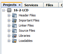
  4. It wont look like mush at the moment, but under Projects on the right, there should now be your newly created project, with a drop down, and a set of folders. Something like this: 
  5. To start the project, we need a main.c. So right click on Source Files, go to New->C Main File... then in the Dialog, change the name to main. After pressing okay, it should look like this: 

Connecting the LCD

LCDs have what is known as a parallel connection. This means that we send data 8 bits at a time, rather than serial where it is one at a time. The datasheet for the PIC is found on the microchip website here. The pinout is found on page 4.

Register Select (RS) pin, this decides which of the two registers that is getting written to. Either the instruction register (what the screen does) or the data register (what is shown on the screen). This is connected to A4 on the PIC.
Read/Write (RW) pin, this decides whether you are writing to or reading from the LCD. This is connected to pin A3.
Enable (E) pin, is to tell the LCD when data needs to be transferred. Pulsing this pin will write or read to the registers the data on the data pins. This is connected to pin  A2.
These pins are defined at the top of the code, to make life easier for us later on.
#define LCD_RS LATAbits.LATA4   //LCD Command/Data Control
#define LCD_RW LATAbits.LATA3   //LCD Read/Write Select
#define LCD_E LATAbits.LATA2    //LCD Enable Line
Data Pins (D0-D7), are the pins that transfer the information between the LCD and the PIC. These are connected to pins B0-B7. So B0 is connected to D0, and so on until B7 is connected to D7.
Vdd and Vss are connected to 5v and GND respectively.
Contrast (Vo) is connected to a 10k pot between the 5v  and  GND.
If the LCD you are using has connections for a backlight, follow the datasheet for instructions, on mine I connect it t0 5v and GND.

The Code

Below is the function I create to send data to the LCD.
#define LCD_CMD 0
#define LCD_TXT 1 

void LCD_DATA (unsigned char data, int type)
{
    __delay_ms(100);   // short delay

    LATB = 0x00;       // reset the register to 0
    LATB = data;       // set B output to the data we want to send
    __delay_ms(1);     // short delay for data to set

    if (type == LCD_CMD)
    {
        LCD_RS = 0;    // command mode
    }
    else
    {
        LCD_RS = 1;    // character/data mode
    }

    LCD_RW = 0;        // start the pulse
    __delay_ms(1);     // small delay
    LCD_E = 1;         // enable LCD data line
    __delay_ms(1);     // small delay
    LCD_E = 0;         // disable LCD data line
    __delay_ms(5);
}
Calling this function in the main, like follows will send data to the LCD. Notice the #define at the top, these are declaring LCD_CMD and LCD_TXT. Basically, when the type is LCD_CMD the LCD is sent into command mode, by setting the RS pin. Equally, sending LCD_TXT will clear the RS pin, putting the LCD in character mode.
The information on the data pins will then get written to the LCD, by clearing RW. To actually tell the LCD that it needs to be sent new instructions the enable pin needs to be pulsed. Once this happens, the screen should be updated with the new information.
#include <stdio.h>
#include <stdlib.h>
#include <xc.h>

#define _XTAL_FREQ 500000

#define LCD_RS LATAbits.LATA4   //LCD Command/Data Control
#define LCD_RW LATAbits.LATA3   //LCD Read/Write Select
#define LCD_E LATAbits.LATA2    //LCD Enable Line

#define LCD_CMD 0
#define LCD_TXT 1 

void LCD_DATA (unsigned char data, int type)
{
    __delay_ms(100);   // short delay

    LATB = 0x00;       // reset the register to 0
    LATB = data;       // set B output to the data we want to send
    __delay_ms(1);     // short delay for data to set

    if (type == LCD_CMD)
    {
        LCD_RS = 0;    // command mode
    }
    else
    {
        LCD_RS = 1;    // character/data mode
    }

    LCD_RW = 0;        // start the pulse
    __delay_ms(1);     // small delay
    LCD_E = 1;         // enable LCD data line
    __delay_ms(1);     // small delay
    LCD_E = 0;         // disable LCD data line
    __delay_ms(5);
}


int main(int argc, char** argv) {
 
    // write "hello world!" on the first line
    LCD_DATA('h', LCD_TXT);
    LCD_DATA('e', LCD_TXT);
    LCD_DATA('l', LCD_TXT);
    LCD_DATA('l', LCD_TXT);
    LCD_DATA('o', LCD_TXT);
    LCD_DATA(' ', LCD_TXT);
    LCD_DATA('w', LCD_TXT);
    LCD_DATA('o', LCD_TXT);
    LCD_DATA('r', LCD_TXT);
    LCD_DATA('l', LCD_TXT);
    LCD_DATA('d', LCD_TXT);
    LCD_DATA('!', LCD_TXT);
 
    while (1)
    {
 
    }
 
 return (EXIT_SUCCESS);
}